Electron-Beam Lithography
Plasmonics, Inc. has the experience and equipment necessary to both prototype and mass produce sub-micron surfaces and devices at industry leading prices. Our expert staff leverages 30 years of fabrication experience and state of the art equipment to provide a variety of lithography services. As a full-service facility, we provide all aspects from concept to production including design consultation. and services (including deposition) are available to assist you through your project.
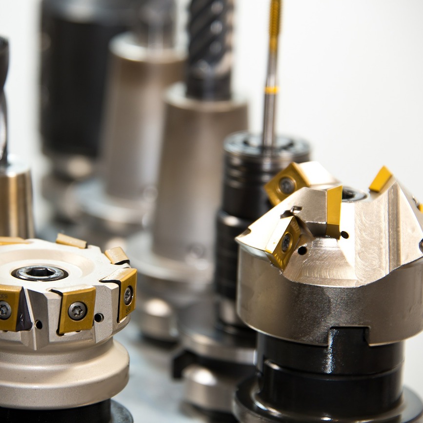
General Fabrication Capabilities
Class 100, 1,000 and 10,000 Clean Room Facilities
Magnetron Sputtering
Electron Beam evaporation
Thermal Evaporation
Oxidation Furnaces
Annealing Furnaces
Reactive Ion Etching
Ion Milling
Contact Lithography
Infrared Sensors & Systems
Our primary focus as a company is extending radio frequency devices into the LWIR and shorter wavelength bands.
Areas of active development:
- Sensors for thermal imaging and smart data collection
- Angle of arrival sensors, focal plane arrays, phased arrays
- Coatings for thermal management and TTL
- Spectral, directional, and polarization control of thermal emission
- Compact infrared optical elements
- Metalens, Reflectarrays, SLMs